EU: Seventh Framework Programme
SNM Project - Single Nanometer Manufacturing for beyond CMOS devices
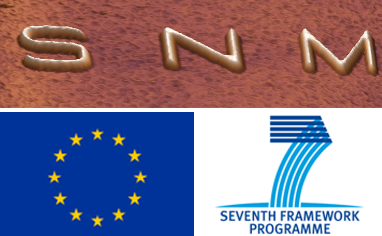
Single Nanometer Manufacturing for beyond CMOS devices
Despite more than 50 years intensive development in Nanotechnology & Micro- and Nanolithography the famous quotation of Richard P. Feynman „There’s Plenty of Room at the Bottom” (1959, at his famous after-dinner talk) is still highly topical. The aim of the Single Nanometer Manufacturing (SNM) project comprises to come very close to this mentioned bottom of nanotechnology, touching the atomic level, which expresses the theoretical limit of constructing nano-systems.
Today, the Si MOSFET (Silicon Metal-Oxide-Semiconductor Field-Effect Transistor) is the backbone of semiconductor electronics and it's scaling, which means the continuous decrease of transistor dimensions, has been the driving force for the last decades of development. This dramatic long-term scaling trend in semiconductor industry is described by the „self-fulfilling prophecy” of Gordon E. Moore, co-founder of Intel, coined afterwards as Moore’s Law. The commitment to Moore’s Law has become a source of inspiration for several technological developments, resulting in an exponential increase of the number of transistors per chip. Following this roadmap the semiconductor industry will break the 10nm scale at the latest end of this decade. However, the working horse of semiconductor industrial manufacturing, the photolithography, is reaching its fundamental physical limitations and the costs of new chip manufacturing fabs are exploding ($50 billion in 2010 for Intel’s 22nm fab).
To maintain Moore’s law in future, keeping the technological evolution alive on which our modern society is based on, novel nano-fabrication technology acts as key enabler to open new horizons in nanotechnology and nanoelectronics. A 15 member strong and diversified team from industry, academia and acclaimed European research institutes, led by TU Ilmenau, Department of Micro- and Nanoelectronic Systems, is drawn together in a single integrated project to achieve this ambitious goal of pushing nano-manufacturing down the single nanometer digit regime and developing methods for precise generation, placement, inspection and integration of such features at the nanoscale. Our approach leverages highly scalable beam based, scanning probe microscopy based & Nanoimprint lithography techniques, emerging science in organic/inorganic molecular based resist materials, advanced nano-pattern transfer techniques, novel inspection and overlay alignment methods and unique processing of novel nano-materials like graphene and MoS2 for integration into novel beyond CMOS nanoelectronic devices. It is the aim of SNM to empower nanotechnology with a clear focus on industrial use, and to drive the rapid development of nano-science leading to new processes and early industrial exploitation of novel nanoelectronic devices like single electron & quantum dot devices.
Laufzeit: 01/2013 - 12/2016
Ansprechpartner:
Prof. Dr. Hans-Werner Schmidt
Lehrstuhl für Makromolekulare Chemie I
E-Mail: hans-werner.schmidt@uni-bayreuth.de
Telefon: + 49 (0)921 55-3200
Dr. Christian Neuber
Lehrstuhl für Makromolekulare Chemie I
E-Mail: christian.neuber@uni-bayreuth.de
Telefon: + 49 (0)921 55-3290
Weiterführende Links: